Wafer Bonding Seal Ring

Different Structures Of Seal Ring Based On Cu Thermo Compression Download Scientific Diagram

Kalrez Bonded Door Seals Offer Significantly Increased Yield And Particle Reduction Benefits In Cvd E O Rings Seals And Custom Molded Rubber Parts Door Seals Seal O Ring

Structures Of Seal Ring Based On Cu Thermo Compression Bonding A 3d Download Scientific Diagram

A Top View Of Three Types Of Microcavities With Metal Sealing Rings Download Scientific Diagram

Top View Of A Sealing Ring Section On The Silicon Wafer After Bonding Download Scientific Diagram

Metal Bonding Based Hermetic Wafer Level Mems Packaging Technology Using In Plane Feedthrough Hermeticity And High Frequency Characteristics Of Thick Gold Film Feedthrough Moriyama 2019 Electrical Engineering In Japan Wiley Online Library

Thara srinivasan lecture 25.
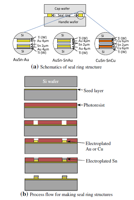
Wafer bonding seal ring. Deposited on patterned si bonding ring. Finally both cap and interposer wafers were bonded together using a wafer to wafer bonder and an adapted ausn soldering process scheme. One such technique is wafer level packaging wlp which forms a hermetically sealed cavity in which the device element is situated. The pair of seal rings for example is arranged in parallel.
Eutectic ausi bonding is the only method where only one joining partner requires a metal frame. The seal ring in one embodiment includes a pair of seal rings i e a first seal ring 150a and a second seal ring 150b. The bond seal area is defined by etching the backside of a cap wafer by 2 µm. Wafer to wafer bonding and packaging dr.
The polymer caps can be implemented through sacrificial etching and a wafer level transfer technique. With advances in wafer bonding technology this process has been widely applied to the fabrication of mems devices. 1 surrounds the main device area 110 and is parallel to the outer perimeter of the die. It is found that the principal cause of the partial bonding is due to non flat bcb sealing ring caused by multilayer bcb coating process.
As a solution bcb dry etching has been proposed to. Metal layer bonding pattern seal rings and bond pads photolithographically eutectic bonding uses eutectic point in metal si phase diagrams to form silicides au and si have eutectic point at 363 c. Here a cap wafer is manufactured with a gold ring metallization and the mems wafer provides a silicon frame area for the metallurgical reaction. Sealing rings after eutectic wafer bonding.
A material a b c d e f cap dicing. Bcb sealing ring has shown partial bonding or full bonding depending on its flatness. This paper presents the effect of bcb sealing ring flatness on bcb bonding for wafer scale bcb cap transfer packaging. The cap wafer was equipped with 200 μm deep dry etched cavities and electro plated au seal rings around them.
These results demonstrate that bonding with the cusn thin film sealing ring at 400 c. Article osti 1107804 title wafer level packaging with compression controlled seal ring bonding author farino anthony j abstractnote a device may be provided in a sealed package by aligning a seal ring provided on a first surface of a first semiconductor wafer in opposing relationship with a seal ring that is provided on a second surface of a second semiconductor wafer and. The seal ring 150 as shown in fig. Due to the concave regions un etched bond rings when the cap wafer comes into a contact with a planar device wafer only the concave seal area un etched area gets bonded.
The bottom wafer generally was a 300µ m thick 4 si wafer having a low bow and a low total thickness variation ttv.

Sanshee Com Store Grey Warden Signet Ring Rings For Men Mens Jewelry Signet Ring
Wax Seal Ring Vintage Ring Rustic Ring Bulky Ring Menly Etsy Mens Rings Fashion Mens Jewelry Wax Seal Ring

Pretty Things Put A Signet On It Diamond Signet Ring Wax Seal Ring Signet Ring
O Ring Yong Leng Trading Co

Antique Vintage 18k Yellow Gold Victorian Designer Cartier Men 39 S Signet Ring Signet Ring Men Signet Ring Mens Jewelry
Https Onlinelibrary Wiley Com Doi Pdf 10 1002 Eej 23193

Satellite Of Love Signet Ring Best Friend Rings Signet Ring Satellite Of Love

A Fine Quality Antique Signet Ring Carved With An English Heraldic Seal This Particular Crest Was Adopt Signet Ring Art Deco Engagement Ring Intaglio Jewelry

Wax Seal Ring Vintage Ring Rustic Ring Bulky Ring Menly Etsy Mens Rings Fashion Wax Seal Ring Rings For Men

O Rings Ptfe

Structure Based On Cu To Cu Thermo Compression Bonding Upper Inset Download Scientific Diagram

Antique Signet Ring Art Nouveau 10k Rosy Yellow Gold 3 Signet Signet Ring Fabulous Jewelry

Pin By Merve Ozcan On Fashion Signet Rings Women Signet Ring Men Signet Ring

Signet Ring Men Gold Carnelian Ring Men Solid Gold Signet Vintage Signet Ring 10k 18k Gold Ruby Man Ring Husband Gift Statement Signet Ring Men Carnelian Ring Rings For Men

Mans Antique Edwardian 10k Gold Carved Signet By Sundayandsunday Men S Jewelry Rings Edwardian Jewelry Edwardian Jewelry Rings

Pin On Rings

Lion Crest Ring Signet Ring Custom Signet Ring Rings For Men

Rubber Sealing Washer Toilet Washer Silicone Cooking Washer Molding Rubber
Https Encrypted Tbn0 Gstatic Com Images Q Tbn 3aand9gctin2kzht2dgcutvsvwv3fmhsmqqdznyqvtp7ri6ag Usqp Cau

This Classic Signet Ring Combines A Bold Chunky Design With Delicate Detailing For A Gorgeous Classy Finish Made From Rings For Men Signet Ring Men S Rings

Men S Fine Estate Jewelry Eragem Signet Ring Signet Ring Men Mens Jewelry

18ct Yellow Gold Signet Ring Oval Small Cat In The Moon Rebus Signet Rings Rebus Signet Rings Dior Ring Signet Ring Silver Jewelry Fashion
Https Ieeexplore Ieee Org Iel7 84 8727545 08699093 Pdf

Apollo Gold Chunky Signet Ring Original Zeus Vintage Gold Coin Signet Ring Queen Elizabeth Ring Family Heritage Gold Ring Gift For Her Gold Coin Ring Signet Ring Gold Rings Gift

Robot Check Signet Ring Men Silver Signet Ring Rings For Men

Silver Signet Ring With Black Onyx Or Carnelian Stone Square Etsy Silver Signet Ring Silver Pinky Ring Signet Ring

Kalrez Bonded Door Seals Offer Significantly Increased Yield And Particle Reduction Benefits In Cvd E O Rings Seals And Custom Molded Rubber Parts Door Seals Seal O Ring

14kt Gold And Diamond Starburst Signet Ring Signet Ring Jewelry Pinky Signet Ring

Man Signet Ring Husband Gift Black Onyx Ring Pinky Ring Black Agate Ring Man Gold Ring Gold Signet Ring Man Onyx Ring Gift For Him Black Onyx Ring Black Agate Ring

Schematics Of The Seal Ring Structure And Production Process Flow Download Scientific Diagram

Baylor University Class Seal Ring Made By University Jewelry At San Jose Jewelers Bayloruniversity Sealrings Class University Rings College Rings Jewelry

Silver Gold Or Platinum Hand Engraved Signet Ring With Your Etsy Rings For Men Signet Ring Fashion Rings

Maison Margiela Silver Signet Ring Silver Signet Ring Morganite Engagement Rings White Gold Sterling Silver Jewelry

James Bond Thunderball Spectre Agent Ring Limited Edition Prop Replica Replica Prop James Bond Bond

Blog Category O Ring Seals O Ring Sizes And Installation

Diamond Lapping Discs Resin Bond Gemstones Glass Artwork
Uk Conical O Ring Mounted Seal Type 13 Type 13 Series Uk Conical O Ring Mounted Seal

Silver Gold Or Platinum Hand Engraved Signet Ring With Your Etsy Signet Ring Silver Signet Ring Hand Engraving

Metallic Alloy Seal Bonding Sciencedirect

Antique Victorian 1890s 14k Gold Ornate Signet Ring Monogram Initials Signet Ring Amazing Jewelry Jewelry Inspiration

Mens Black Onyx Ring Onyx Signet Ring Gold Mens Ring Blackstone Ring Vintage D1979 Mens Retro Ring Mens Pinky Ring Black Stone Ring Onyx Signet Ring Black Stone Ring Black Onyx
Perfluoroelastomer Ffkm O Rings Global O Ring And Seal